
Antenna design in small spaces
Designing antennas for compact products means looking at the whole device: the PCB, enclosure, battery, shields, connectors and other radio frequency circuits all change how the antenna behaves.
In many electronic products, the antenna shares space with the battery, display, connectors, shields, metal parts of the enclosure and other RF circuits. All of these can shift its resonant frequency, efficiency and radiation pattern.
At ECK we have worked with a range of PCB antennas and chip antennas. In one development, for example, we had to integrate three antennas into a device roughly the size of a credit card, one of them covering two frequency bands for Wi-Fi and GPS.
This article brings together some practical notes on choosing, placing, laying out and testing antennas in compact electronic products.
Antenna design: fundamentals and behavior
Put simply, an antenna converts between electrical signals and electromagnetic fields.
In a transmitter, the electrical signal travels along the transmission line to the antenna, where part of the energy is converted into an electromagnetic wave.
In a receiver, the opposite happens: the electromagnetic energy picked up by the antenna is converted into an electrical signal that goes to the receiving circuit.
In practice, however, an antenna’s behavior depends heavily on the environment in which it is installed.
Radiation pattern and directivity
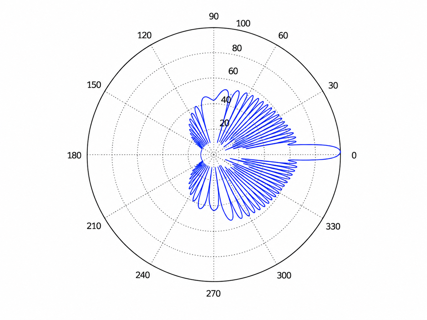
One important characteristic is how energy is radiated into space.
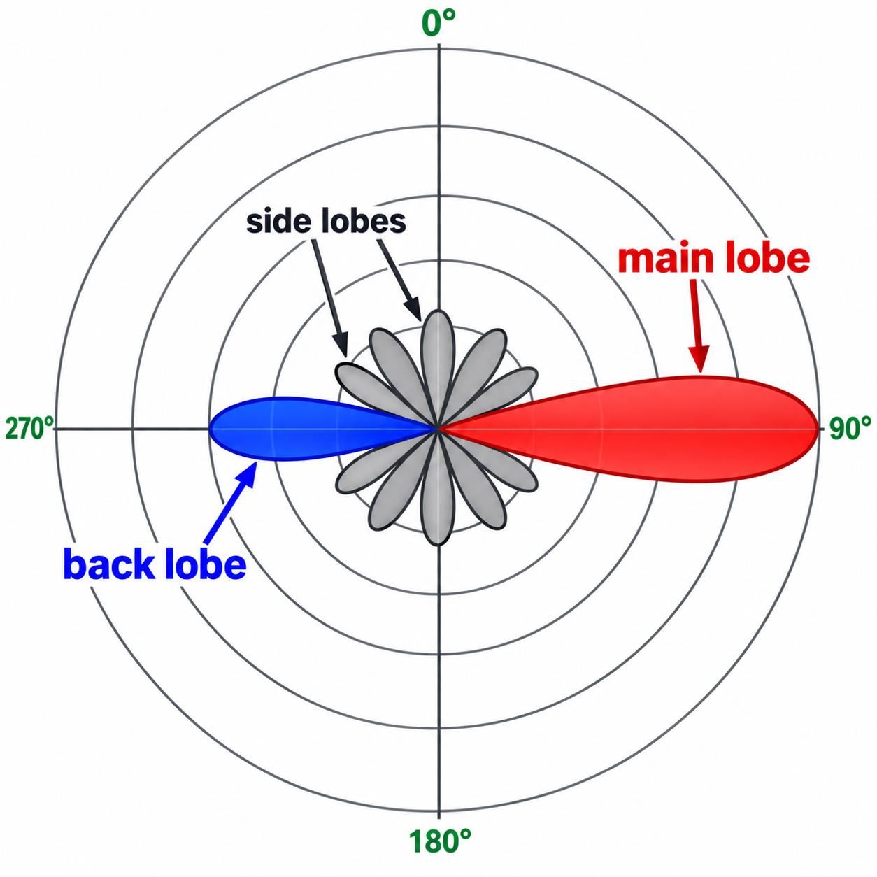
An antenna can have a main lobe, side lobes and a back lobe. This means two antennas with similar gain figures can behave very differently depending on the direction in which you want to transmit or receive.
So, besides gain, it is important to check directivity and the radiation pattern.
A GPS patch antenna, for example, has very different characteristics from an antenna designed to radiate more evenly around the device.
What to consider when choosing an antenna
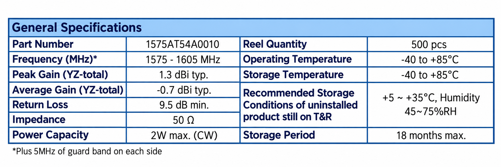
Antenna selection should take the complete product into account, not just the operating frequency.
The main factors include efficiency, gain, bandwidth, directivity, physical size, required ground plane, position on the PCB and how the antenna behaves once installed in the final enclosure.
You also need to assess the frequency range the antenna actually covers.
In compact products, an antenna with a wider operating band can be more tolerant of the shifts caused by mechanics, enclosure materials and nearby components.
The enclosure affects the antenna
The antenna should not be analyzed separately from the mechanics.
Plastic materials, wall thickness, screws, metal brackets, batteries, shields and other nearby components can change the resonant frequency and efficiency.
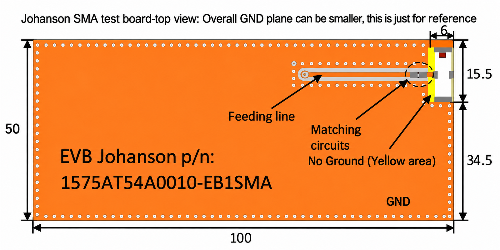
That is why an antenna that works correctly on the manufacturer’s evaluation board may behave differently once installed in the final product.
Whenever possible, validation should be done with the board mounted in the position where it will be used and inside the final enclosure.
Antenna position and component placement
Component placement on the PCB also affects performance.
A rule of thumb is to keep tall components and metal parts away from the antenna area, especially when the manufacturer specifies a keep-out area or a region without a ground plane.
Some antennas are designed to sit at the edge of the board. Others can be placed elsewhere, as long as the ground plane and the manufacturer’s recommendations are respected.
Manufacturers usually provide evaluation boards and reference designs showing dimensions, GND area, copper-free region, feed line and matching circuit.
These documents are a good starting point for the layout.
PCB size is part of the antenna too
In many designs, especially with chip antennas, the PCB ground plane is directly part of how the antenna works.
So making the board much smaller or larger than the manufacturer’s reference can change tuning and efficiency.
This effect is particularly important when you try to reuse the same antenna model in devices of very different sizes.
The influence of the operating environment
The product must be evaluated under real operating conditions.
Some antennas change their behavior when the device is close to the human body, to metal structures or to other materials with different dielectric properties.
Choosing an antenna is therefore a trade-off between space, cost, efficiency, range and real installation conditions.
Components for RF circuits
The components used in the RF circuit also deserve attention.
In matching circuits, it is advisable to use components suited to the operating frequency and to look at characteristics such as stability, tolerance and high-frequency behavior.
Even a capacitor with the same nominal value as a generic part can behave differently at RF.
That is why supplier and component selection should be part of the design strategy.
Two parts of the antenna system
An antenna design can be split into two main parts:
1. The electrical path between the transmitter or receiver and the antenna, including transmission line, connectors and matching circuit.
2. The conversion between the electrical signal and the electromagnetic wave, determined by the antenna and its surroundings.
This split helps explain why a system can show good VSWR and still have lower-than-expected range.
RF line impedance
Transmitters, receivers, transmission lines and antennas are usually designed to work with a defined characteristic impedance, often 50 ohms.
When there is an impedance mismatch between points along the RF path, part of the energy is reflected.
To reduce this, a matching circuit may be needed, often a pi network or another topology suited to the application.
The key is to provide footprints in the layout for the components needed to allow tuning during testing.
How to measure VSWR
A practical way to assess antenna matching is to measure VSWR with an impedance analyzer or equivalent instrument.
The aim is to see how the antenna behaves across the frequency range and find where the best match occurs.
In the project shown below, a vector impedance analyzer was used to check a Johanson 1575-series antenna.
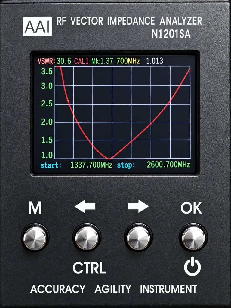
The measurement should be made as close as possible to the final product configuration.
That includes the enclosure, battery, connectors, cables and other mechanical parts near the antenna.
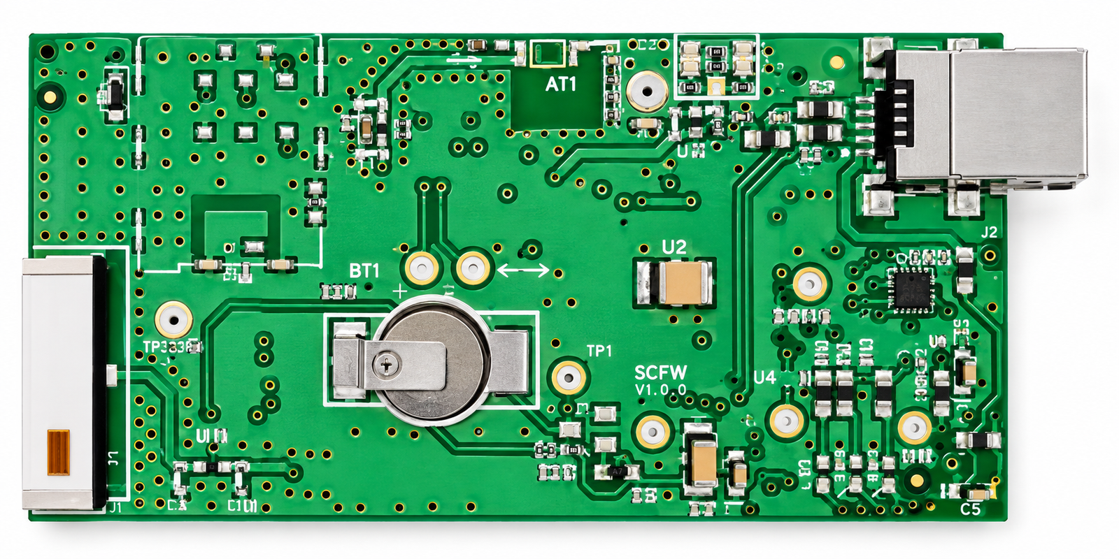
Testing on a project board
In this example, the antenna showed its best point near 1637 MHz, while the band of interest stayed within a region considered usable by the VSWR criterion adopted in the development.
At that stage, the final enclosure was not yet available.
So the final antenna tuning would be done later, with the final mechanics assembled.
Component positions were also left in the matching circuit to allow tuning.
How to achieve low VSWR
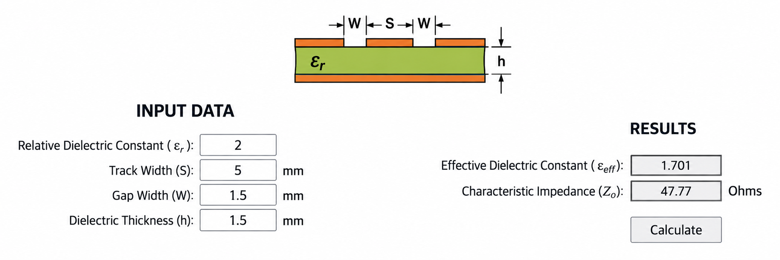
The first step is to make sure the line between the RF circuit and the antenna has the correct impedance.
This depends on trace width, distance to the ground plane, laminate thickness and dielectric constant, and the structure used on the PCB.
There are calculators that help size microstrip and coplanar waveguide lines.
Here, a coplanar waveguide calculator was used to estimate the line geometry required.
Tuning circuit
It is advisable to physically provide the antenna tuning circuit even if, on the first prototype, some components are fitted as shorts or left unpopulated.
This allows tuning to be corrected later without requiring an immediate PCB revision.
In the project mentioned, small SMD components were used in the tuning circuit, keeping the RF area compact.
RF layout: keep the line simple
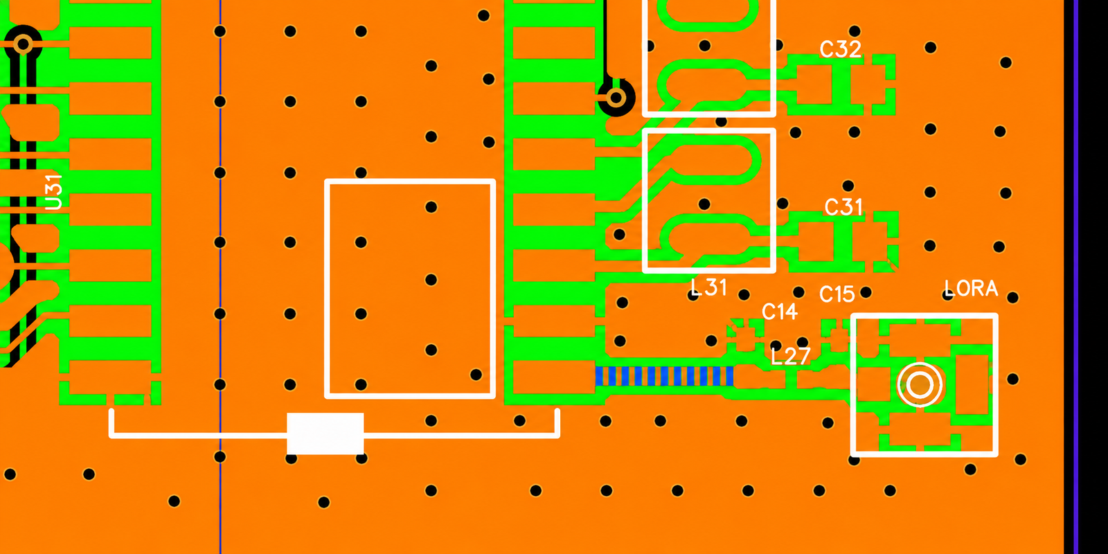
In RF, unnecessarily long paths, sharp changes of direction and discontinuities should be avoided.
In the LoRa layout example below, the antenna line runs straight to the U.FL connector, with no unnecessary detours.
GND vias can also be placed along the line to help contain the electromagnetic field and improve the behavior of the transmission structure.
VSWR is not the same as efficiency
It is important to separate two concepts.
VSWR helps assess the impedance match of the assembly.
Efficiency indicates how much of the energy actually delivered to the antenna is converted into useful radiation.
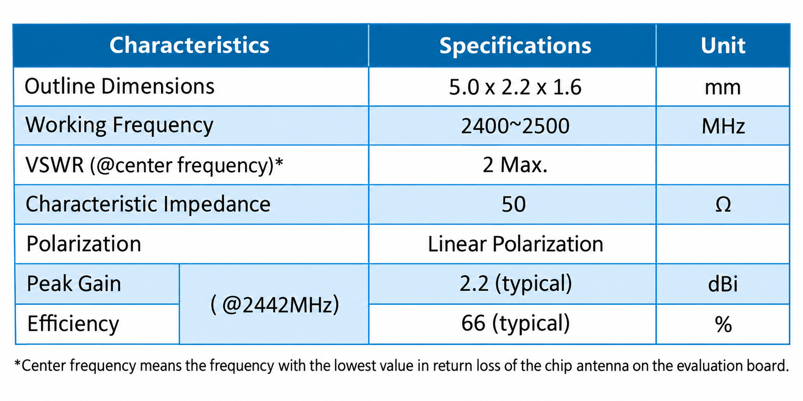
An antenna can show an apparently good VSWR and still perform poorly because of nearby metal parts, enclosure properties, an inadequate ground plane or other effects of the final product.
So the analysis should not stop once VSWR is within the desired range.
How to assess efficiency in practice
A simple comparison method is to use an RF source and a field strength measurement setup.
You can generate a signal with a reference antenna and measure its strength at a given distance.
Then repeat the same test with the antenna installed in the device, keeping conditions as similar as possible.
This comparison does not replace a professional anechoic chamber measurement, but it can help identify significant performance differences during development.
When VSWR is fine and range is still poor, it is worth investigating the effect of the mechanics, the ground plane and components near the antenna.
Using an SDR during development
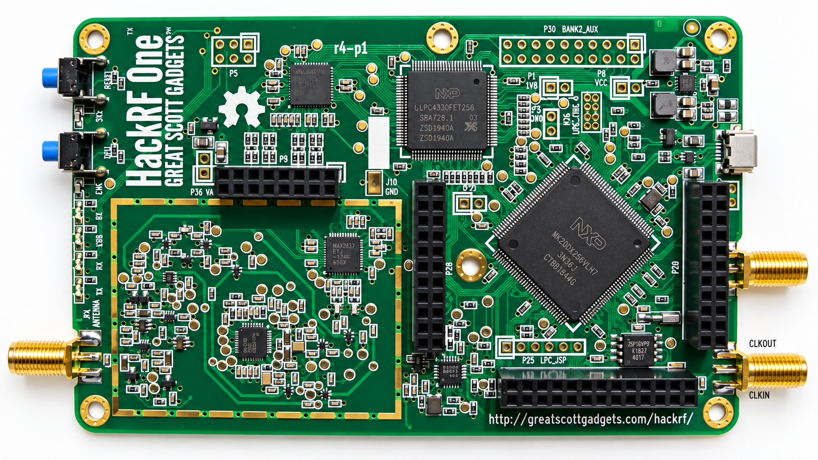
An SDR can be a useful bench tool for viewing signals, checking the spectrum and supporting many tests during RF system development.
The HackRF One is one example of a tool used for this kind of analysis.
Conclusion
Designing an antenna into a compact device requires looking at the whole assembly.
It is not enough to choose an antenna based on the frequency and gain listed in the datasheet.
You need to consider the ground plane, position on the PCB, transmission line, matching circuit, enclosure, battery, metal parts and the real operating environment.
A good strategy is to start from the manufacturer’s recommendations, provide tuning options on the first prototype and take measurements with the product increasingly close to its final configuration.
This reduces the risk of discovering range or stability problems only in the final stages of development.
In products with Wi-Fi, Bluetooth, GPS, LoRa and other radio interfaces, space is usually tight and the different systems have to coexist within the same mechanics.
That is why antenna, RF, PCB and mechanics should be treated as parts of the same design.
For complete projects, see ECK’s electronic product development service.
Have an electronic product to develop?
Tell us the problem. The conversation starts with engineering, not with an off-the-shelf package.