
PCB surface finish: HASL, ENIG or OSP?
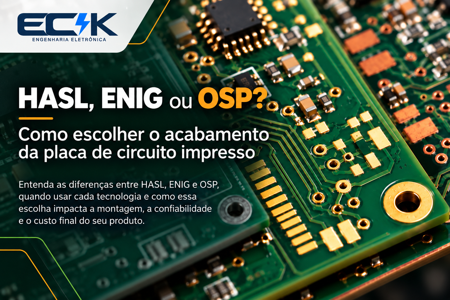
Choosing a PCB surface finish is often treated purely as a price decision. However, a relatively small saving on PCB fabrication can lead to much higher costs in assembly, inspection, rework and even field service.
As electronic components get smaller and packages have ever closer terminals, the quality and uniformity of the solder pad surface become increasingly important.
That is why choosing between HASL, ENIG and OSP should not depend only on the price quoted by the board fabricator. You need to consider the components used, the assembly process, production volume, storage conditions and the product’s reliability requirements.
Why does the PCB surface finish matter?
After the board is fabricated, the copper surfaces intended for soldering must be protected against oxidation until assembly. The surface finish does this while also providing a surface suitable for soldering the components.
This choice affects pad flatness, solderability, board storage, the ability to rework, assembly of fine-pitch components, production repeatability and the cost of both the PCB and the assembly.
In prototypes or small batches, some differences may go unnoticed. When production ramps up, however, small process issues can turn into hundreds of reworks. That is when the apparently cheapest option may no longer be the lowest-cost solution.
HASL: the traditional, economical option
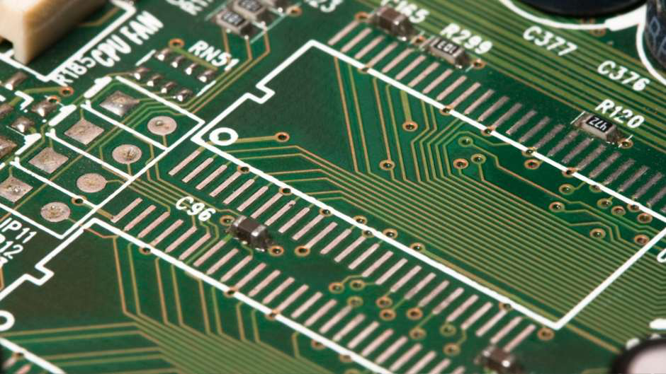
HASL (Hot Air Solder Leveling) is one of the most traditional finishes used in printed circuit board fabrication. In this process, the copper surface receives a layer of solder alloy and the excess is removed with hot air knives.
There are leaded HASL processes and lead-free versions, used to meet the substance restrictions of the RoHS directive. Its main advantage is relatively low cost, and it is widely available among PCB fabricators.
On the other hand, the resulting surface is not perfectly flat. Solder layer thickness can vary across different areas of the board. For conventional components this is usually not a significant problem. But as pitch and terminal dimensions shrink, flatness becomes more important for assembly quality and repeatability.
ENIG: a flat surface with good oxidation protection
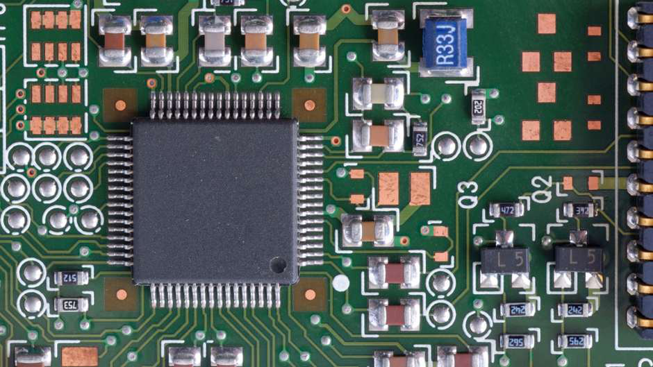
ENIG (Electroless Nickel Immersion Gold) uses a nickel layer over the copper followed by a thin layer of gold. The nickel acts as a barrier between the copper and the surface, while the gold protects the nickel against oxidation before assembly.
One of ENIG’s main advantages is a very flat, uniform surface. This makes it particularly attractive for boards with fine-pitch components and packages where pad uniformity matters for the assembly process.
Another advantage is good shelf life when the fabrication process and packaging conditions are adequate. The cost is usually higher than HASL, but in some products the reduction in assembly problems and rework can make up for the difference.
OSP: an organic coating on the copper
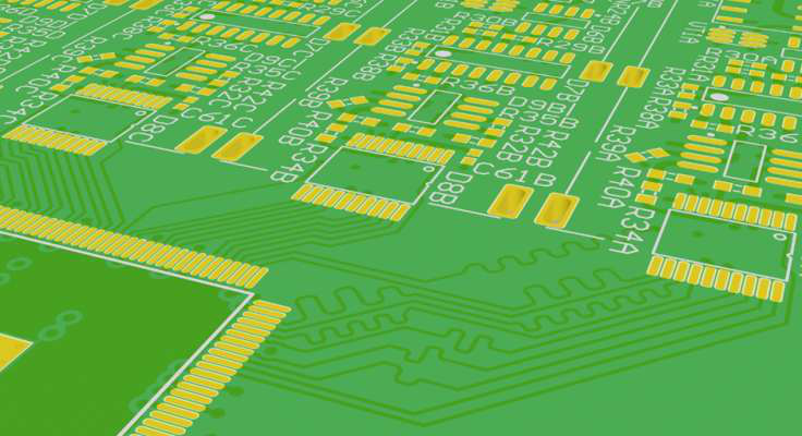
OSP (Organic Solderability Preservative) uses an organic film applied to the copper to protect it against oxidation between PCB fabrication and assembly.
During soldering, this layer is removed by the thermal and chemical action of the process, allowing the solder joint to form. An important feature of OSP is excellent flatness, since no significant metal layer is deposited on the pads.
This makes it suitable for high-density assembly and can be an economically attractive option in series production. On the other hand, storage and handling require tighter control, and its use should be assessed together with the product’s fabrication and assembly process.
Cold joints and poor wetting are not the same thing
Problems seen during assembly do not always have the same cause. A cold solder joint occurs when the conditions needed to properly form the solder joint are not adequately reached.
A joint that looks visually acceptable, on the other hand, may have wetting problems or an incomplete metallurgical bond between the solder and the surfaces involved. Oxidation, contamination, an inadequate thermal profile, incorrect PCB storage and the characteristics of the surface finish can all contribute to these problems.
With lead-free processes, assembly temperatures are also higher than in traditional leaded processes. Simply raising the oven or soldering iron temperature may not fix the root cause and can expose components and PCB to more thermal stress.
What about BGA and fine-pitch components?
The smaller the terminals and the spacing between them, the more important surface uniformity tends to be. Packages such as BGA, QFN and fine-pitch SMD components require a much more tightly controlled assembly process than conventional components.
In these cases, PCB finish, stencil, solder paste, thermal profile, component storage and inspection must be treated as parts of the same production system. A cheaper PCB that increases the defect rate can quickly eat up the savings made when buying the boards.
HASL, ENIG or OSP: which one to choose?
There is no universally best finish. HASL can be an economical and suitable solution for a large number of products, especially when there are no critical flatness requirements.
ENIG offers excellent flatness and surface protection and is often a good choice for higher-density designs with fine-pitch components. OSP also offers great flatness and can bring cost advantages in series production, as long as storage, handling and the assembly process are compatible with its characteristics.
Choosing the right PCB surface finish therefore depends on the product and the production process, not just on the price difference between the options offered by the board fabricator.
PCB cost is not product cost
In electronic product development, shaving a little off the cost of a board can look like an obvious decision when you look only at the bill of materials. But the real cost involves much more: PCB + assembly + inspection + testing + rework + production losses + field service.
A cheaper fabrication option can turn out more expensive when assessed across the product’s full life cycle. That is why the PCB surface finish specification should be part of the engineering decisions made during hardware development.
See also our electronic engineering projects. At ECK Electronic Engineering, we look at these decisions considering not only how the circuit works, but also fabrication, assembly, testing and the product’s viability in production.
Need to develop or review an electronic product?
ECK works on hardware development and on analyzing fabrication and assembly problems.